
What are Semiconductors?
Semiconductors are materials with conductivity in between conductors (usually metals) and non-conductors or insulators (such as ceramics). Semiconductors are made up of compounds like gallium arsenide or pure elements like germanium or silicon. The theories, properties, and mathematical techniques that govern semiconductors are explained in physics.
Examples of Semiconductors:
Some of the most often used semiconductors include gallium arsenide, germanium, and silicon. Silicon is used in the manufacturing of electronic circuits, while gallium arsenide is used in solar cells, laser diodes, and other applications.
Table of Content
Holes and Electrons in Semiconductors
Mobility of Electrons and Holes
The mobility of electrons in a semiconductor is greater than that of holes. It's mostly due to the fact that their band structures and scattering mechanisms are so different.
The conduction band is where electrons travel, while the valence band is where holes travel. Due to their restricted movement, holes cannot travel as freely as electrons when an electric field is applied.
In semiconductors, holes are formed when electrons are raised from their inner shells to higher shells. Because the nucleus exerts a stronger atomic force on holes than on electrons, holes have less mobility.
If the effective mass of the particles is less and the time between scattering events is longer, a particle's mobility in a semiconductor is greater.
The mobility of electrons in intrinsic silicon at 300 K is 1500 cm2 (Vs)-1, while the mobility of holes is 475 cm2 (Vs)-1.
You may like to read about LED:
The electron bond model in valency 4 of silicon is shown below. A hole is created when one of the free electrons (blue dots) leaves the lattice position (grey dots). This hole, which has the opposite charge as the electron, can be thought of as a positive charge carrier moving in the lattice.

Concept of Electrons andHoles in Semiconductors
Band Theory of Semiconductors
The quantum revolution in science resulted in the advent of band theory. The energy bands were discovered by Walter Heitler and Fritz London.
The electrons in an atom are known to exist in several energy levels. When we want to create a solid lattice with N atoms, each atom's level must be separated into N levels in the solid.
Energy Bands are formed by the splitting up of acute and tightly packed energy levels. A Band Gap is the space between consecutive bands that represent a range of energies with no electron.

Energy Band Diagram for Semiconductors, Conductors, and Insulators
Conduction Band and Valence Band in Semiconductors
Valence Band:
Conduction Band:
The energy levels of positive (holes) or negative (free electrons) charge carriers are included in the lowest unoccupied band. It has conducting electrons, which cause electricity to flow. The conduction band is generally vacant and has a high energy level. In semiconductors, the conduction band takes electrons from the valence band.
Properties of Semiconductors
Semiconductors have the ability to conduct electricity under preferable conditions. This distinguishes it as a great material for conducting electricity in a controlled manner.
In contrast to conductors, charge carriers in semiconductors are created only by external energy (thermal agitation). It causes a certain number of valence electrons to jump into the conduction band and cross the energy gap, leaving an equal number of vacant energy states, i.e. holes. The importance of electron and hole conduction is equal.
- Conductivity: 105 to 10-6 mho/m
- Current Flow: Due to electrons and holes
- Temperature coefficient of resistance: Negative
- Resistivity: 10-5 to 106 Ωm
Why does the resistivity of Semiconductors go down with Temperature?
The difference in charge carrier density between conductors and semiconductors causes the difference in resistivity. Because the quantity of charge carriers increases rapidly as temperature rises, the resistivity of semiconductors decreases, making the fractional change i.e. negative temperature coefficient NTC.
Some Important Properties of Semiconductors are:
- At zero Kelvin, a semiconductor serves as an insulator. It acts as a conductor when the temperature rises.
- Semiconductors can be doped to make semiconductor devices suited for energy conversion, switches, and amplifiers due to their exceptional electrical properties.
- There are fewer power losses.
- Semiconductors are smaller and lighter than transistors.
- They have higher resistivity than conductors but a lower resistivity than insulators.
- When the temperature rises, the resistivity of the semiconductor materials decreases, and vice versa.
Types of Semiconductors
Semiconductors are classified into two types:
- Intrinsic Semiconductor
- Extrinsic Semiconductor


Intrinsic Semiconductor

Chemically, an intrinsic form of semiconductor material is made to be very pure. There's only one type of element in it.
The most common intrinsic semiconductor elements are germanium (Ge) and silicon (Si). They have four electrons in their valence shell (tetravalent). At absolute zero temperature, they form a covalent bond with the atom.
Due to collisions, a few electrons become unbounded and free to migrate around the lattice as the temperature rises, resulting in an absence in its initial position (hole). The conduction of electricity in the semiconductor is aided by these unbound electrons and holes. The number of negative and positive charge carriers is equal.
Thermal energy could only ionize a few atoms in the lattice, resulting in lower conductivity.
The Lattice of Pure Silicon Semiconductor at Different Temperatures
- At absolute zero Kelvin temperature: At this temperature, the covalent bonds are extremely strong, and there are no free electrons, making the semiconductor a perfect insulator.
- Above absolute temperature: As the temperature rises, a small number of valence electrons leap into the conduction band, making it a poor conductor.
Energy Band Diagram of Intrinsic Semiconductor
An intrinsic semiconductor's energy band diagram is shown below:
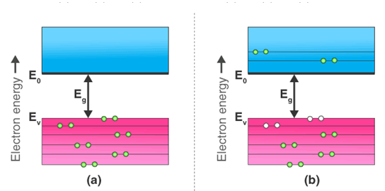
Current flows in intrinsic semiconductors due to the migration of free electrons and holes. The total current is equal to the sum of the electron current (Ie) due to thermally generated electrons and the hole current Ih
Total Current (I) = Ie + Ih
The probability of electrons existing in the conduction band is an intrinsic semiconductor drop exponentially with increasing bandgap at finite temperature (Eg)
n = n0e-Eg/2.Kb.T
Where,
- Eg = Energy bandgap
- Kb = Boltzmann’s constants
Extrinsic Semiconductor
By introducing a small number of suitable replacement atoms are known as IMPURITIES, the conductivity of semiconductors can be considerably increased. DOPING is the process of introducing impurity atoms into a pure semiconductor. In a doped semiconductor, only 1 out of every 107 atoms are replaced by a dopant atom. Extrinsic semiconductors are further divided into the following categories:
- N-type Semiconductor
- P-type Semiconductor
 Classification of Extrinsic Semiconductor
- Mainly due to electrons
- Entirely neutral
- I = Ih and nh >> ne
- Majority – Electrons and Minority – Holes
When a pentavalent impurity (P, As, Sb, Bi) is doped into a pure semiconductor (Silicon or Germanium), four of the five valence electrons link with the four electrons of Ge or Si.
The dopant's fifth electron is freed. As a result, the impurity atom is known as "Donar" since it donates a free electron for lattice conduction.
The negative charge carriers increase when the number of free electrons increases due to the addition of an impurity. As a result, it is known as an n-type semiconductor.
The donor atom creates an immobile positive ion, although the crystal as a whole is neutral. Because a significant number of free electrons are required for conduction, electrons in an n-type semiconductor are the MAJORITY CARRIERS, whereas holes are the MINORITY CARRIERS.
- Mainly due to holes
- Entirely neutral
- I = Ih and nh >> ne
- Majority – Holes, and Minority – Electrons
When a pure semiconductor is doped with a trivalent impurity (B, Al, In, Ga), the impurity's three valence electrons bond with three of the semiconductor's four valence electrons.
This results in the absence of an electron (hole) in the impurity. These impurity atoms are known as "Acceptors" because they are ready to accept bound electrons.
As the amount of impurities rises, so do the number of holes (positive charge carriers). As a result, it's known as a p-type semiconductor.
The acceptors become stationary negative ions, and the crystal as a whole is neutral. Because a significant number of holes are required for conduction, the holes in a p-type semiconductor are MAJORITY CARRIERS, while electrons are MINORITY CARRIERS.
You may like to read about LED:
Let's look at how semiconductors are used in everyday life. Almost all electronic gadgets contain semiconductors. Our lives would be very different if they didn't exist.
Their reliability, compactness, low cost, and control of electricity conduction make them perfect for a variety of applications in a wide range of components and devices. Semiconductors are used to make transistors, diodes, photosensors, microcontrollers, integrated chips, and much more.
- Semiconductor devices are used to make temperature sensors.
- They are utilized in 3d printing technology.
- Microchips and self-driving automobiles use it.
- Calculators, solar plates, computers, and other electronic equipment use this material.
- Semiconductors are utilized to make transistors and MOSFETs, which are employed as switches in electrical circuits.
Industrial Uses of Semiconductors
Semiconductors' physical and chemical properties enable them to create modern wonders such as microchips, transistors, LEDs, and solar cells.
Transistors and other regulating devices composed of semiconductor materials make up the microprocessor used to regulate the operation of space vehicles, railroads, robots, and other systems.
Importance of Semiconductors
We've covered some of the advantages of semiconductors, which make them quite helpful in a wide range of applications.
§ They are highly portable due to their tiny size
§ They require less input power
§ Semiconductor devices are shockproof
§ They have a longer lifespan
§ They operate without making any noise
0 Comments
Send us a query